


Driven by exponential expansion in AI compute infrastructure and data center deployments, alongside rapid industrial rollout of 800G/1.6T optical transceivers and CPO architectures, silicon photonic chips are entering a high-volume production boom. Wafer-level testing, a foundational mass manufacturing step, now faces drastically elevated requirements for throughput, measurement consistency and operational stability. Fully automated test platforms have become a critical solution to break testing bottlenecks holding back silicon photonics commercialization, while delivering a flexible, competitive hardware option for global fabs seeking diversified test equipment suppliers.
As a long-standing specialist in semiconductor test equipment, Semishare addresses critical pain points across the silicon photonics value chain via proprietary in-house technologies, launching a fully automated wafer-level silicon photonic test platform optimized for high-volume device manufacturing. Centered on an automated probe station, the platform integrates 6-axis ultra-precision positioning stages, optical coupling assemblies, optoelectronic probes, machine vision modules, and complete measurement hardware & software suites.
Boasting end-to-end automation, tightly integrated high-precision hardware, and broad device compatibility, Semishare delivers streamlined, accurate, adaptable test workflows to help silicon photonics manufacturers worldwide cut operational costs and scale production efficiency. The system features native interoperability with mainstream optoelectronic testers from Keysight, Advantest and other leading vendors, enabling turnkey mass-production test stacks such as Semishare + Keysight or Semishare + Advantest. This flexible ecosystem equips global manufacturers with a wide selection of scalable test configurations tailored for high-volume silicon photonic fabrication.
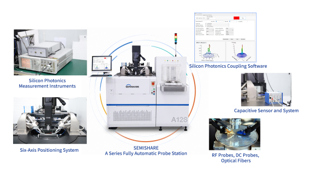

Nanometer-precise alignment – making optical coupling easy
Silicon photonic chip optical waveguides are extremely small in size, and the alignment precision between the probe and the waveguide directly affects test loss and yield. Semishare's fully automated wafer-level silicon photonic test system employs self-developed optical alignment and closed-loop control technologies. Leveraging the high-speed, stable motion performance of the fully automated probe station and the precise positioning of the nano-piezoelectric coupling stage, it achieves nanometer-scale high-precision coupling between the optical probe and the silicon photonic waveguide, boosting coupling efficiency by over 30% and ensuring test accuracy. Meanwhile, the real-time Z-axis height monitoring system prevents probe damage to the chip. The chuck offers fA-level leakage current and 0.1°C high-precision temperature control (supporting 25°C to 150°C, with other temperatures customizable), enabling simulation of chip operating conditions across multiple application scenarios. Together, these features ensure test stability and chip safety from the ground up, effectively resolving yield fluctuation challenges.
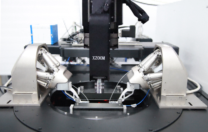

High-precision fully automated probing – streamlining test workflows and maximizing efficiency
To address the inefficiencies and reliance on manual labor in traditional testing, Semishare's fully automated wafer-level silicon photonic test system features a self-developed pre-alignment module that enables damage-free automatic wafer loading/unloading and high-speed transfer, supporting 24/7 continuous on-wafer testing. With parallel test and stacked test modes, it can test multiple chips simultaneously, significantly boosting test throughput. In addition, dedicated accessories and custom fixtures greatly shorten pre-test setup time.
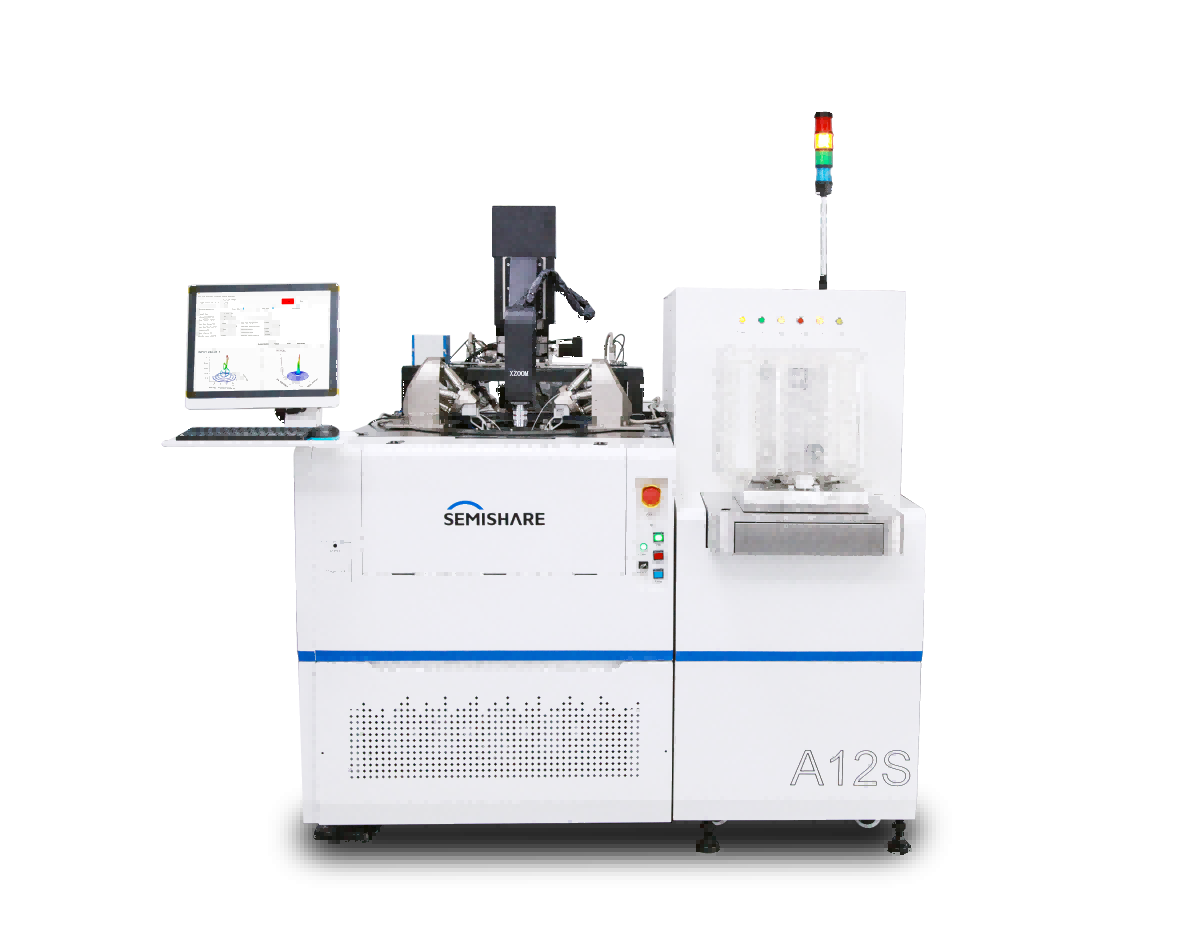
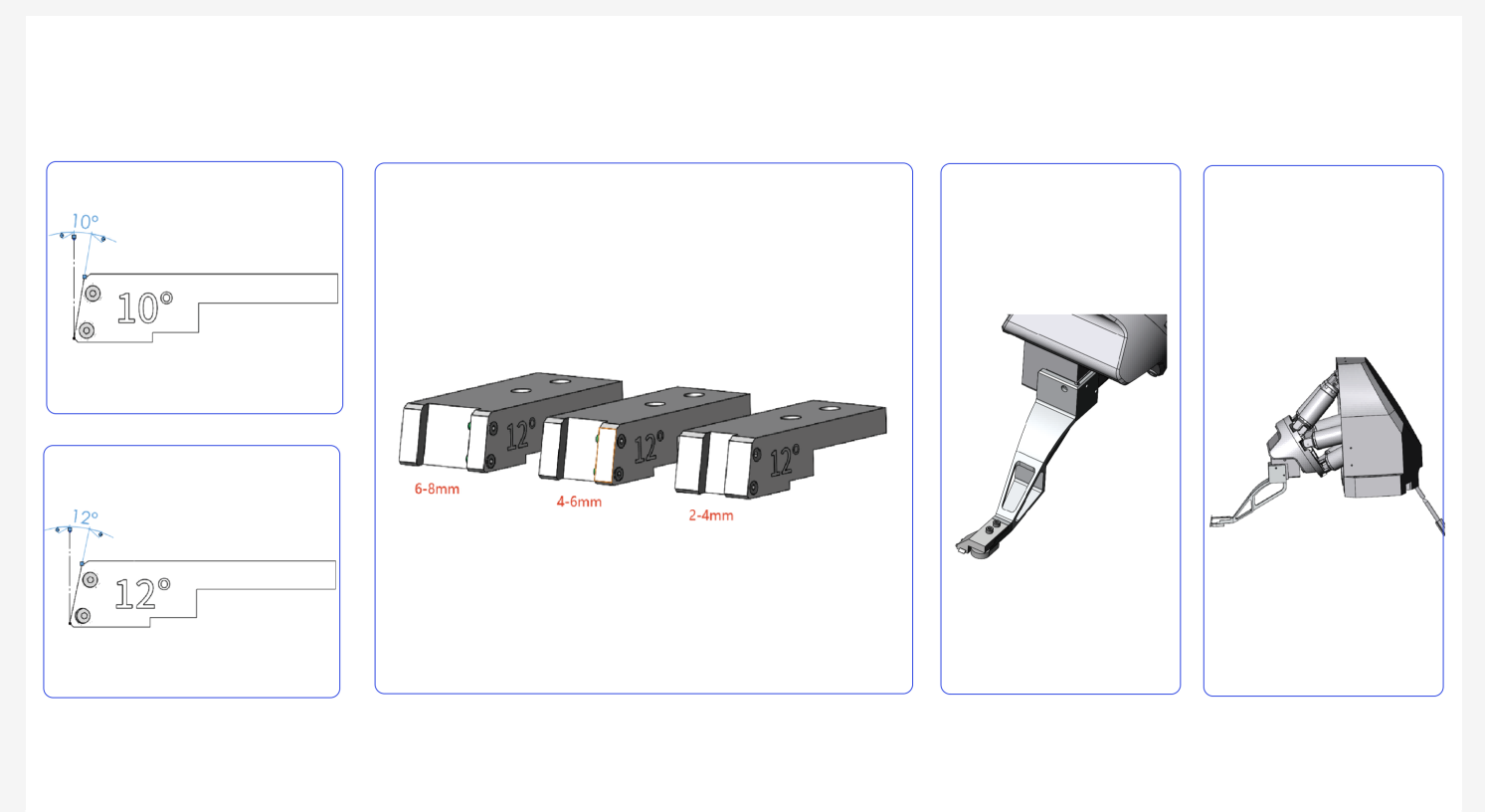
Modular design. Flexible coupling. Lower capital costs
To address the challenge of diverse test scenarios and poor adaptability of traditional equipment, the system features a modular, scalable design that fully supports both wafer-level edge coupling and vertical coupling, compatible with single-fiber and fiber-array configurations. A single system covers the vast majority of silicon photonic chip test scenarios. It supports customizable wavelengths (O-band & C-band) and 1-to-32 channel fiber arrays, compatible with single-mode and polarization-maintaining fibers, and adaptable to various standard and special pitch specifications. With a range of custom fixture options, the system accommodates different wafer sizes and multiple product generations, significantly reducing costly duplicate equipment investments.
Integrated software for full-process automation and closed-loop data management
Semishare's fully automated test software and PTS™ integrated system deliver end-to-end automation and closed-loop data management for the entire test workflow. The graphical user interface simplifies operation, while automated alignment and calibration functions minimize human errors. The PTS™ software supports multi-site parallel testing, flexible test item configuration, and seamless integration with mainstream test instruments. It automatically saves, consolidates, and analyzes test data, generates reports based on customizable templates, and provides open data export interfaces – forming a complete "test – analyze – optimize" closed loop that delivers critical data support for process refinement and yield improvement.
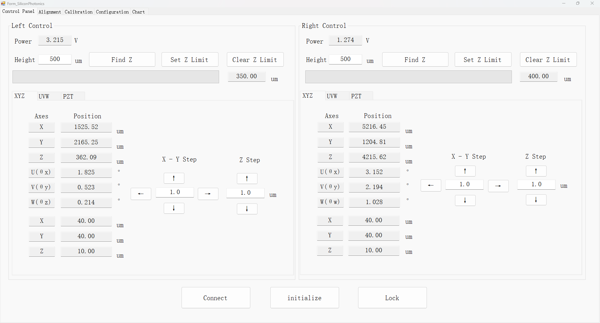
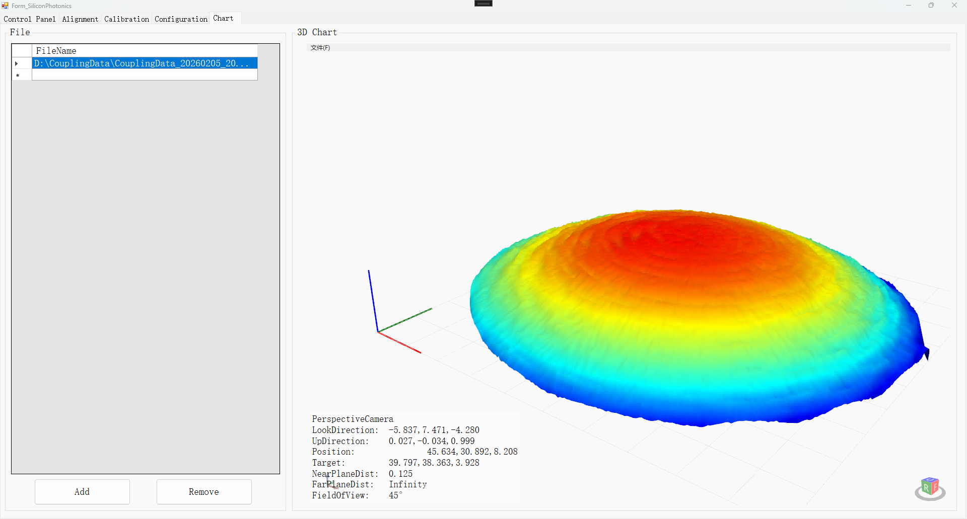
Fully Automated Test Software
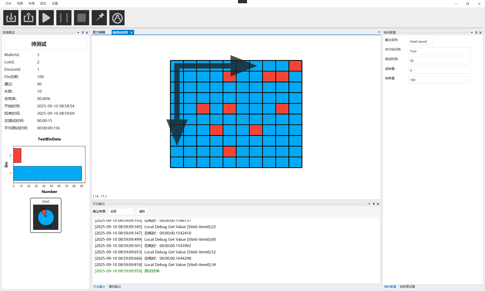
PTS™ Software
Against a backdrop of fast-tracked commercial scaling across the silicon photonics sector, global demand for fully automated wafer-level test platforms keeps rising steadily. SEMISHARE’s newly released Fully Automated Wafer-Level Silicon Photonics Test System addresses unmet market needs for dedicated silicon photonic testing hardware. Backed by standout technical performance and customizable service packages, the platform delivers a high-competitiveness testing alternative for silicon photonics manufacturers worldwide. Having already been deployed at multiple chip fabrication facilities, the solution has earned broad recognition across the industry.
Moving forward, SEMISHARE will further deepen its R&D capabilities in silicon photonics test technology, closely track global technical evolution, and continuously overcome key technical limitations. Drawing on our independently developed proprietary hardware technology, we aim to equip silicon photonics manufacturers with reliable, high-performance testing infrastructure, advancing higher precision and throughput standards for the global silicon photonics ecosystem.