
Test Solution

Optoelectronic devices use light-electrical conversion effects made of various functional devices; optical devices can be divided into photoelectric chips, optical devices, and optical modules. The types of photoelectric devices are photovoltaic tubes, photomultiplier tubes, photoresistors, photodiodes, phototransistors, photocells, photocouplers, LEDs (light-emitting diodes), LDs (laser diodes) and photodetectors.
Optoelectronic performance testing usually includes the following aspects:
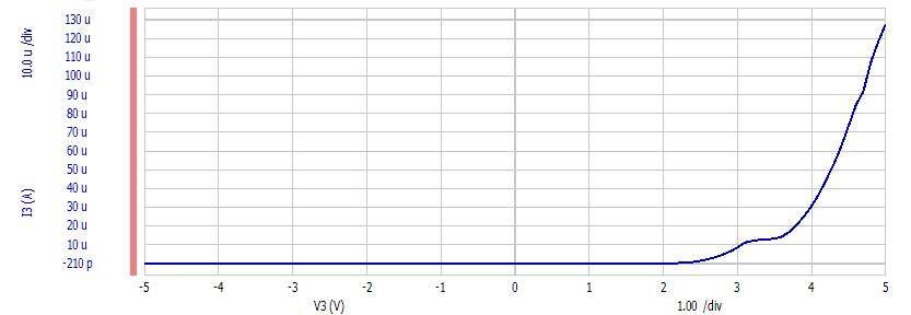
1.Photoelectric response characteristics test: by providing a light source to the photoelectric device, measure its response to light signals, including photocurrent, photovoltage, photoelectric conversion efficiency and other test parameters.。
2.Spectral Characterization Test: Measure the response of the photoelectric device in different wavelength ranges to understand its sensitivity and selectivity to different wavelengths of light signals.
3.Device parameter test: including the test of the optoelectronic device's resistance, capacitance, inductance and other electrical parameters to evaluate its electrical properties.
4.Response time test: Measure the response speed of the optoelectronic device to the optical signal, including the test of rise time, fall time and other parameters.
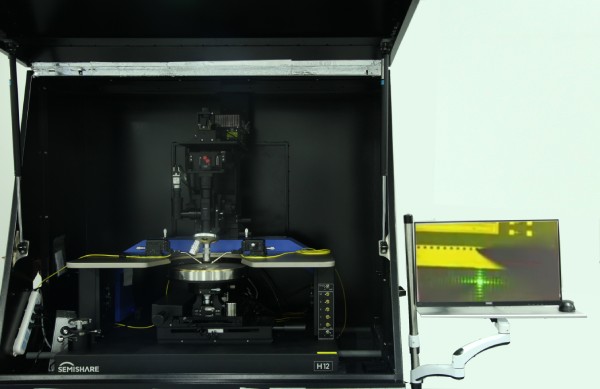
The current widespread difficulty lies in how to efficiently conduct testing at the level of optical chips.When testing optical chips, issues such as low coupling efficiency, high coupling loss, and a lack of automation in testing schemes have become common concerns. Among them, stress testing under non-working conditions requires ensuring a long period of high and low-temperature environments. For Micro-LED high-density integrated LED arrays, with pixel distances on the order of 10 micrometers, a high-resolution, high-magnification microscope is required.Precision is crucial for components like probes and probe holders.
>SEMISHARE---SS-100 MicropositionerLearn More
>SEMISHARE----H Series Integrated Manual Probe StationLearn More
micro LED
Movement accuracy 0.7μm, leakage accuracy within 10pA
1、The wafer will be placed on the chuck to open the vacuum adsorption, put on rubber gloves to move the wafer slightly to confirm that the adsorption is firm;
2、After adjusting the chuck air-controlled movement, smooth placement of the central position to the bottom of the microscope;
3、In the selection of the appropriate objective lens to adjust the focus until the wafer clear image is shown on the display;
4、Operate the probe seat to adjust the probe position so that the probe is accurately tied to the corresponding PAD;
5、Check the conductivity of the fixture cable and the tester's connection; after connecting the PN pole of the sample point, apply current or voltage.
1、Accurate and fast positioning of the test points
2、After testing, accurate and fast movement to the next test point
3、Smooth pneumatic-driven movement operation
 Request for quotation

0755-2690 6952 turn 801/804/806/814
 Send Email
